
In the ever-changing world of technology, the semiconductor business is at the center, powering the devices we use daily. Key sectors in the semiconductor ecosystem like Outsourced Assembly and Testing (OSAT) and Assembly Testing Marking and Packaging units (ATMPs) have appeared, making it easier to make and test chips in an efficient way. This blog post talks about how important the Semiconductor Chip Packaging Industry is, how the market works, how new jobs are opening up, and what skills are needed in this exciting area.
Understanding OSAT and ATMP
When it comes to making semiconductors, OSAT (Outsourced Semiconductor Assembly and Test) is all about sending chip packing and testing to service providers who are experts in those areas. These companies take care of the last steps of making semiconductors. For example, they package and test the chips to ensure they work well and meet quality standards. On the other hand, ATMP stands for “Assembly, Testing, Marking, and Packaging.” This is assembling integrated circuits, testing them carefully, marking them with important information, and then packaging them for distribution. In short, OSAT and ATMP are very important parts of making semiconductors.
Let’s Understand with an example-
Let’s look at a real-world example to see how important OSAT and ATMP are in the semiconductor business (see Figure 1). Imagine a company that specializes in making cutting-edge integrated circuits (ICs) for microprocessors. But instead of making these ICs themselves, they work together with a company called Y-FAB. This partnership lets them focus on creation while outsourcing the process of making things. Here are the steps that help us understand the whole process:
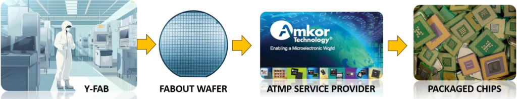
Step-I
Y-FAB is a well-known fabrication plant that makes a lot of wafers for different customers every month. Most of the time, their main job is to make semiconductor chips with multiple microprocessor ICs on them. But when it comes to putting each chip in its own package, they use a special service called an ATMP facility. This important part of the process is taken care of by these companies. (for example Amkor Technologies).
Step-II
After Y-FAB makes the wafers, they send them to an ATMP service provider. This company focuses on putting together, testing, labeling, and packing semiconductor chips. At the ATMP building, the chips are carefully packaged to keep them safe and make sure they work right. Flip-chip bonding, wire bonding, and other advanced techniques like Fan-out Wafer-level packaging and System-in-Package (SiP) are used during this process.
Step-III
Also, the chips go through a lot of testing at the ATMP center to make sure they work well, are reliable, and are of good quality. During this testing process, the chips go through a variety of tests, like stress testing, temperature testing, and electrical verification, to make sure they meet the industry’s strict standards.
Final Step
After being packed and tested, the chips are sent back to Y-FAB. The fab then sends these packaged and tested chips to the microprocessor company. The microprocessor company can then use them in their final goods or give them to their customers.
This process between the microchip company Y-FAB and the ATMP service provider shows how important OSAT and ATMP are for making the process of making semiconductors more efficient. By using the knowledge of specialized service providers, the microprocessor company can focus on what it does best, which is designing chips. At the same time, it can use the ATMP facility’s efficient and reliable packaging and testing services.
The Market and Job Opportunities
The Semiconductor Chip Packaging Industry market has grown very quickly in recent years. This is because semiconductor chips are increasingly used in many different businesses. Also, the rise of smartphones, tablets, car electronics, Internet of Things (IoT) devices, and AI technologies has increased the need for high-quality, advanced semiconductors in a big way.
Industry Insight
Industry sources say that in 2020 the Semiconductor Chip Packaging Industry market was worth about $35 billion. It is also expected to hit over $50 billion by 2025, with an annual growth rate of about 8%. Because of this growth, there are now a lot of different job opportunities in this field. In the same way, the market for ATMP is also projected to grow. This prediction is based on the fact that computer chips are getting more complicated and smaller.
Job opportunities
With this kind of market growth, there are a lot of job possibilities in the OSAT and ATMP industries. As an example, the table shows some important jobs and the average yearly salaries that Indians can expect for them. Notably, it’s important to note that only a few companies in India, like ingotSEMI, offer specific training and workshops for these highly technical jobs.
| Job Title | Job Function | Expected Salary |
| Packaging Engineers | Designing and implementing the packaging solutions for semiconductor chips, considering factors like thermal management, electrical performance, and reliability | 7-10 LPA (Beginners)
12-20 LPA (Experienced) |
| Test Engineers | Design and implementation of a comprehensive test plan | 6-10 LPA (Beginners)
10-15 LPA (Experienced) |
| Process Engineers | optimizing and improving the assembly and testing processes | 7-10 LPA (Beginners)
12-20 LPA (Experienced) |
| Quality Assurance Specialists | maintaining strict quality control standards, conducting failure analysis, and implementing corrective actions | 7-10 LPA (Beginners)
12-20 LPA (Experienced) |
| Equipment Technicians | operating and maintaining the advanced machinery and equipment used in the packaging and testing processes | 5-7 LPA (Beginners)
8-10 LPA (Experienced) |
Since we’ve already discussed the different jobs in the Semiconductor Chip Packaging Industry, it’s important to know what skills each work requires. Now, let’s talk about the skills that Packaging Engineers, Test Engineers, Process Engineers, and Quality Assurance Specialists need to have in order to do their jobs well. By doing this, we can learn more about the skills that are needed for these jobs.
IC Packaging Engineers
To do well in these jobs, you need to have education and skills like:
- Foundational requirements include getting a degree in Electrical Engineering, Materials Science, or a related area.
- It is important to know about different ways to package semiconductors, like flip-chip, wire bonding, and more modern methods like System-in-Package (SiP) and Fan-out Wafer Level Packaging.
- Knowing how to use CAD software for package design is a useful skill.
Knowing about thermal control, electrical performance, and reliability regarding IC packaging is important. - To stay compliant, knowing the industry norms and rules for IC packaging is important.
Test Engineers for Semiconductor Chip Packaging Industry
These roles required certain qualifications, and skills are necessary, including:
- Attaining a degree in Electrical Engineering, Electronics, or a related field serves as a fundamental requirement.
- Demonstrating proficiency in test methodologies, test equipment handling, and test program development is crucial.
- Possessing knowledge of semiconductor device physics and integrated circuit functionality is essential.
- Gaining experience with various testing techniques, such as functional testing, parametric testing, and burn-in testing, is highly valuable.
- Exhibiting strong analytical and problem-solving skills specifically related to the Semiconductor Chip Packaging Industry is important.
Process Engineers for Semiconductor Chip Packaging Industry
- Attaining a degree in Chemical Engineering, Electrical Engineering, or a related field is a foundational requirement.
- Demonstrating an understanding of semiconductor manufacturing processes, including lithography, etching, deposition, and wafer fabrication, is crucial.
- Possessing proficiency in process optimization, yield improvement, and statistical process control (SPC) is highly beneficial.
- Having knowledge of the Semiconductor Chip Packaging Industry is essential to navigate the industry’s dynamics effectively.
- Familiarity with process simulation and modeling software is advantageous for analyzing and optimizing manufacturing processes.
Quality Assurance Specialists for Semiconductor Chip Packaging Industry
- Obtaining a degree in Electrical Engineering, Quality Engineering, or a related field is a foundational requirement.
- Possessing knowledge of quality management systems, methodologies, and tools specific to IC Packaging is crucial.
- Having an understanding of statistical analysis and quality control techniques is highly valuable.
- Gaining experience with failure analysis methods and root cause analysis is important in maintaining quality standards.
- Demonstrating strong attention to detail and the ability to implement quality standards and processes is necessary for ensuring product integrity and reliability.
Equipment Technicians for Semiconductor Chip Packaging Industry
- Obtaining an associate degree or technical diploma in Electronics, Electrical Engineering Technology, or a related field is a foundational requirement.
- Demonstrating proficiency in operating and maintaining semiconductor testing and assembly equipment is crucial.
- Possessing troubleshooting skills to diagnose and resolve equipment malfunctions is highly valuable.
- Having knowledge of equipment calibration procedures and preventive maintenance is important for equipment reliability and accuracy.
- Understanding safety protocols and adhering to cleanroom practices is essential for maintaining a safe working environment.
Please note that specific skill requirements may vary depending on the company, level of experience, and the complexity of the semiconductor devices being handled. Continuous learning and staying updated with industry advancements are crucial for success in these roles within the fast-paced semiconductor industry.
0 Comments